TLDR;
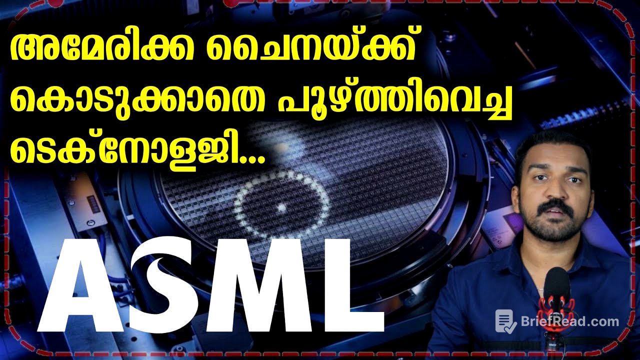
This video tells the story of ASML, a Dutch technology company that has become a key player in the semiconductor industry. ASML is the only company in the world that can produce Extreme Ultraviolet (EUV) lithography machines, which are essential for manufacturing advanced microchips. These machines use EUV light to etch incredibly small patterns on silicon wafers, enabling the creation of smaller, more powerful transistors. The development of EUV technology was a major challenge, requiring breakthroughs in light generation, optics, and vacuum engineering. ASML's success has had a profound impact on modern technology, enabling advancements in smartphones, laptops, AI, and more. However, the company's dominance has also made it a key player in global geopolitics, particularly in the technology competition between the United States and China.
- ASML is the sole producer of EUV lithography machines, essential for advanced microchip manufacturing.
- EUV technology enables the creation of smaller, more powerful transistors, driving advancements in various industries.
- The development of EUV lithography was a complex and costly undertaking, requiring significant investment and collaboration.
- ASML's technology has made it a key player in global geopolitics, particularly in the US-China technology competition.
Introduction to ASML [0:00]
ASML, a Dutch technology company, stands as a pivotal force in the semiconductor industry. It possesses the unique knowledge and technical prowess to construct highly sophisticated machinery capable of etching patterns on silicon at a scale smaller than a virus. These machines, costing over $150 million per unit and representing thousands of man-years of effort, are poised to revolutionize the semiconductor industry.
The Challenge of Shrinking Transistors [1:00]
Advancements in computers and phones are slowing down due to limitations in creating smaller transistors. Moore's Law, which states that the number of transistors on a microchip doubles approximately every two years, is becoming increasingly difficult to maintain as transistors shrink to the point where they can no longer fit on chips. The challenge lies in lithography, a process that uses stencils and light to etch shapes on silicon chips.
The Advent of EUV Lithography [2:31]
For years, engineers have used Deep Ultra Violet (DUV) light for lithography, but its wavelength of 193 nanometers has limitations. To overcome this, scientists turned to extreme ultraviolet (EUV) light, which has a much shorter wavelength of 13.5 nanometers. EUV light enables the etching of smaller shapes on silicon, allowing for more transistors to fit on a chip.
Overcoming the Challenges of EUV Light [3:28]
EUV light is not readily available in nature and must be produced in the laboratory by recreating conditions similar to those inside a star. This involves shining a high-energy laser beam into droplets of molten tin, which then turns into plasma and emits EUV light. Controlling EUV light is also challenging because it is easily absorbed by glass and air. To address this, scientists developed special mirrors made of thin layers of materials that reflect EUV light without absorbing it. The entire process must be conducted in a vacuum to prevent the air from interfering with the EUV light.
The Complexity of EUV Machines [6:17]
Each EUV machine is the size of a bus, weighs over 180 tons, and contains more than 100,000 components. The assembly process is incredibly complex, requiring the collaboration of thousands of engineers, distributors, and scientists from around the world. Each machine takes over a year to complete. Despite the complexity and cost, EUV technology enables the engraving of patterns on chips at seven nanometers or less.
ASML's Journey to Commercialization [6:54]
ASML's journey to commercializing EUV lithography was fraught with setbacks. Early prototypes were unreliable, and the company spent billions of dollars on research and development. To overcome these challenges, ASML formed partnerships with major semiconductor companies like Intel, TSMC and Samsung, who provided financial support and valuable feedback. After nearly 30 years of effort and over nine billion dollars in investment, ASML finally achieved a breakthrough, with the first commercial EUV machines rolling off the production line in 2016.
The Impact of EUV Technology [8:11]
EUV lithography has had a transformative impact on the semiconductor industry. TSMC used EUV lithography to build chips that power advanced AI models like those in iPhones, PlayStation 5, and Chat GPT. By 2020, ASML had become the backbone of an $800 billion industry. Each EUV machine is worth over $150 million, and ASML has a market capitalization of over $300 billion. ASML's technology affects almost every aspect of modern life, including smartphones, laptops, electric vehicles, cloud computing, and medical devices.
ASML's Future and Geopolitical Implications [9:10]
ASML is working on next-generation lithography technology known as HiNAUV, which promises even smaller transistors and greater computational power. However, ASML's dominance has also made it a key player in global geopolitics. The semiconductor industry is at the center of technology competition between the United States and China. The US has imposed strict export restrictions to prevent ASML from selling EUV machines to China, putting ASML in a difficult position as it tries to maintain its role as a neutral supplier. ASML is dedicated to its work and has not only revolutionized the semiconductor industry but also inspired a new generation of inventors.


![So You Want to Be an ANESTHESIOLOGIST [Ep. 12]](https://wm-img.halpindev.com/p-briefread_c-10_b-10/urlb/aHR0cDovL2ltZy55b3V0dWJlLmNvbS92aS96OGgxbVJxSTNfSS9ocWRlZmF1bHQuanBn.jpg)