
TLDR;
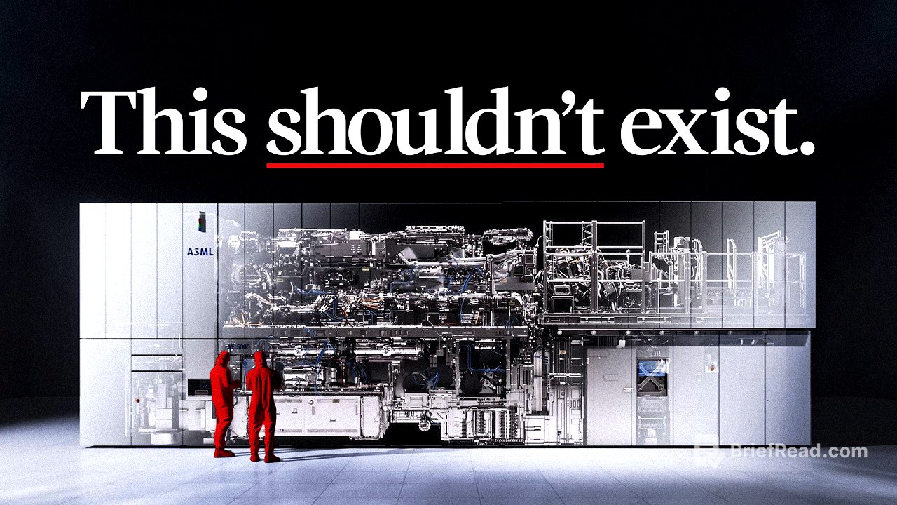
This video explores the intricate world of microchips, specifically focusing on the technology that has enabled the continuation of Moore's Law and the advancements in chip production. It delves into the advancements made by the company ASML, including the production processes of microchips, the evolution of extreme ultraviolet (EUV) lithography, and the significance of ASML in the tech industry.
- Microchips consist of billions of transistors, and smaller transistors allow for faster and more powerful chips.
- The production of microchips involves complex processes including photolithography and multiple layers of fabrication.
- Extreme ultraviolet lithography is crucial for producing smaller features on chips and is a revolutionary technology developed by ASML.
The Machine That Saved Moore’s Law [0:00]
Microchips, central to modern technology, are essentially intricate systems built from billions of transistors. As transistors have shrunk over the years, their ability to double in number every two years showcases Moore's Law, a trend identified by Gordon Moore in 1965. However, progress stagnated around 2015 until a $400 million machine revolutionised chip manufacturing. This machine uses lasers to precisely interact with tiny droplets of molten tin, achieving extraordinary exactness in the layering process for microchips.
How are microchips made? [3:12]
The microchip creation process begins with purifying silicon dioxide from sand into nearly pure silicon. A seed crystal is then immersed in molten silicon, leading to the growth of a silicon ingot, which is sliced into wafers. Each wafer undergoes polishing and is coated with a light-sensitive material called photoresist, before being exposed to light through a patterned mask. This process creates detailed imprints of chip designs, followed by etching and metal deposition to form electrical connections. The cycle of coating, exposing, etching, and depositing is repeated for each layer of the microchip, typically ranging from 10 to 100 layers.
What is extreme ultraviolet lithography? [9:11]
Extreme ultraviolet (EUV) lithography represents a significant evolution in chip manufacturing by utilising much shorter wavelengths for photolithography, enabling the printing of increasingly miniature features. The process has encountered various challenges due to diffraction limits and material absorption. Japanese scientist Hiroo Kinoshita proposed using x-rays but faced hurdles regarding electron ejection from materials. Eventually, multi-layer mirrors were developed to reflect x-rays, leading to proof of concept for x-ray lithography. However, the practical application required overcoming significant obstacles in creating an efficient light source and smooth enough mirrors for precise lithography.
Nuclear Fusion To The Rescue [15:04]
The Lawrence Livermore National Lab, originally established for nuclear weapons research, began exploring x-ray light production from nuclear fusion reactions. This x-ray light could potentially aid in lithography. Over time, Andrew Hawryluk from this lab applied insights to develop x-ray lithography further, but faced skepticism and challenges in gaining acceptance for his ideas. Despite initial backlash, partnerships with significant labs and government funding facilitated advancements.
How ASML Conquered The Chip World [21:59]
ASML emerged as a leader in semiconductor manufacturing by focusing on EUV technology. Initially a small company, ASML made strategic partnerships to develop the required optics and sources essential for EUV lithography. This collaboration with Zeiss led to innovative breakthroughs in mirror design and the eventual selection of optimal wavelengths for maximum reflectivity. Despite setbacks and financial needs leading to investment from major chip producers, ASML dedicated itself to the pursuit of building a commercially viable EUV lithography machine.
Who are ASML’s biggest customers? [35:35]
ASML's main customers include prominent companies like Intel, Samsung, and TSMC, who rely on ASML's technology to maintain their competitive edge in semiconductor production. The significant investments from these companies illustrate the crucial dependence of the semiconductor industry on ASML's innovations and technology. Orders for ASML's EUV machines surged as they became pivotal to producing advanced, efficient chips.
The Most Important Tech Company In The World [37:40]
ASML is positioned as a critical tech company globally because its machines enable the production of the latest generations of microchips, which underpin all modern electronic devices. The company's EUV machines, essential for making smaller and more powerful chips, are highly sought after in the industry, establishing ASML’s influence over future technology advancements.
Inside ASML [41:25]
The video provides an inside look at ASML's production facilities, which maintain stringent cleanliness requirements necessary for fabricating sensitive chips. The complex assembly process of ASML's machines involves a multitude of components and careful oversight to ensure quality and performance. The high standards for precision reflect the intricate manufacturing needed to lead in semiconductor technology. The video concludes by highlighting the immense challenges and perseverance involved in achieving breakthroughs that seemed initially impossible.